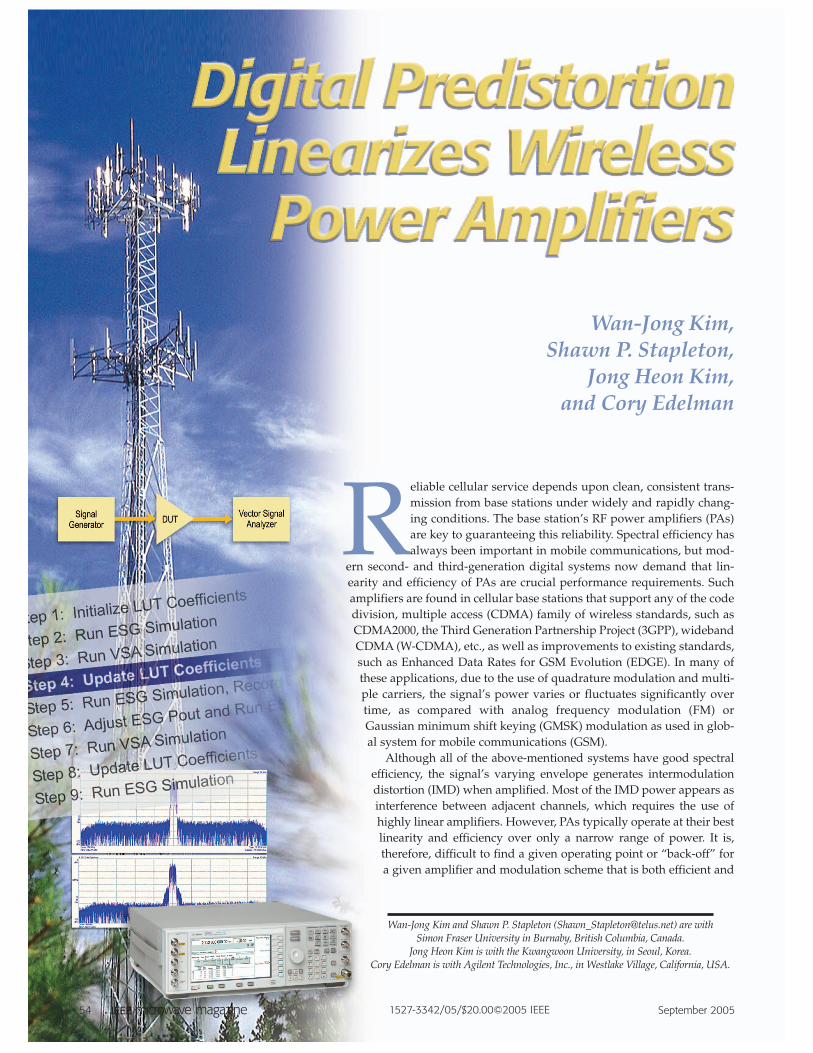
wan-jong kim, shawn p. stapleton, jong heon kim, and...
TRANSCRIPT
54 September 20051527-3342/05/$20.00©2005 IEEE
Wan-Jong Kim,Shawn P. Stapleton,
Jong Heon Kim,and Cory Edelman
Wan-Jong Kim and Shawn P. Stapleton ([email protected]) are withSimon Fraser University in Burnaby, British Columbia, Canada.
Jong Heon Kim is with the Kwangwoon University, in Seoul, Korea.Cory Edelman is with Agilent Technologies, Inc., in Westlake Village, California, USA.
Reliable cellular service depends upon clean, consistent trans-mission from base stations under widely and rapidly chang-ing conditions. The base station’s RF power amplifiers (PAs)are key to guaranteeing this reliability. Spectral efficiency hasalways been important in mobile communications, but mod-
ern second- and third-generation digital systems now demand that lin-earity and efficiency of PAs are crucial performance requirements. Suchamplifiers are found in cellular base stations that support any of the codedivision, multiple access (CDMA) family of wireless standards, such asCDMA2000, the Third Generation Partnership Project (3GPP), widebandCDMA (W-CDMA), etc., as well as improvements to existing standards,such as Enhanced Data Rates for GSM Evolution (EDGE). In many ofthese applications, due to the use of quadrature modulation and multi-ple carriers, the signal’s power varies or fluctuates significantly overtime, as compared with analog frequency modulation (FM) orGaussian minimum shift keying (GMSK) modulation as used in glob-al system for mobile communications (GSM).
Although all of the above-mentioned systems have good spectralefficiency, the signal’s varying envelope generates intermodulationdistortion (IMD) when amplified. Most of the IMD power appears asinterference between adjacent channels, which requires the use ofhighly linear amplifiers. However, PAs typically operate at their bestlinearity and efficiency over only a narrow range of power. It is,therefore, difficult to find a given operating point or “back-off” fora given amplifier and modulation scheme that is both efficient and
September 2005 55
free of distortion products, e.g., linear operation. Also,backing-off the power into an amplifier lowers powerefficiency and increases heat dissipation, both of whichare highly undesirable effects in the confined space of abase-station shelter. To further complicate things, notethat a CDMA-type base station’s signal will changedepending upon the instantaneous number of users inthe cell. In practice, linearity can be improved at theexpense of efficiency or through the use of linearizationtechniques. In this article, we will present a detailedlook at one such approach known as digital predistor-tion (DP). This will be implemented, for our purposes,using electronic design automation (EDA) sofware con-nected to standard laboratory test equipment. Let usfirst review some of the available linearization tech-niques and compare them.
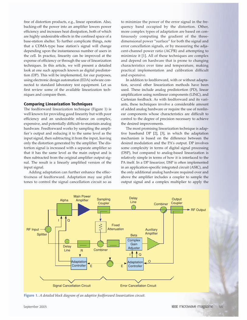
Comparing Linearization TechniquesThe feedforward linearization technique (Figure 1) iswell known for providing good linearity but with poorefficiency and an undesirable reliance on complex,expensive, and potentially difficult-to-maintain analoghardware. Feedforward works by sampling the ampli-fier’s output and reducing it to the same level as theinput signal, then subtracting it from the input, leavingonly the distortion generated by the amplifier. The dis-tortion signal is increased with a separate amplifier sothat it has the same level as the main output and isthen subtracted from the original amplifier output sig-nal. The result is a linearly amplified version of theinput signal.
Adding adaptation can further enhance the effec-tiveness of feedforward. Adaptation may use pilottones to control the signal cancellation circuit so as
to minimize the power of the error signal in the fre-quency band occupied by the distortion. Other,more complex types of adaptation are based on con-tinuously computing the gradient of the three-dimensional power “surface” for both the signal anderror cancellation signals, or by measuring the adja-cent-channel power ratio (ACPR) and attempting tominimize it [1]. All of these techniques are complexand depend on hardware that is prone to changingcharacteristics over time and temperature, makingpractical implementation and calibration difficultand expensive.
In addition to feedforward, with or without adapta-tion, several other linearization methods have beenused. These include analog predistortion (PD), linearamplification using nonlinear components (LINC), andCartesian feedback. As with feedforward and its vari-ants, these techniques involve a considerable amountof added analog hardware or require the use of nonlin-ear components whose characteristics are difficult tocontrol to the degree of precision necessary to achievethe desired improvements.
The most promising linearization technique is adap-tive baseband DP [2], [3], in which the adaptationmechanism is based on the difference between thedesired modulation and the PA’s output. DP involvessome complexity in terms of digital signal processing(DSP), but compared to analog-based linearization isrelatively simple in terms of how it is interfaced to thePA itself. In a DP linearizer, DSP is often implementedin an application-specific integrated circuit (ASIC), andthe only additional analog hardware required over andabove the amplifier includes a coupler to sample theoutput signal and a complex multiplier to apply the
Figure 1. A detailed block diagram of an adaptive feedforward linearization circuit.
RF Input
Splitter
AlphaMain Power
Amplifier SamplingCoupler
FixedAttenuation Auxiliary
Amplifier
DelayLine
DelayLine
Combiner
OutputCoupler
RF Output
Error Cancellation CircuitSignal Cancellation Circuit
E
RI Q
I Q
O
Combiner
Beta
ComplexGain
Adjuster
EAdaptationController
AdaptationController
56 September 2005
PD. As a result, DP is less costlyto implement than feedforward.In addition, the effectiveness ofDP does not, unlike the feedfor-ward or analog PD techniques,depend on the operating fre-quency of the system. It is, there-fore, particularly well-suited forsoftware-defined radio applica-tions, in which a single set of RFhardware is used to cover a widerange of frequencies.
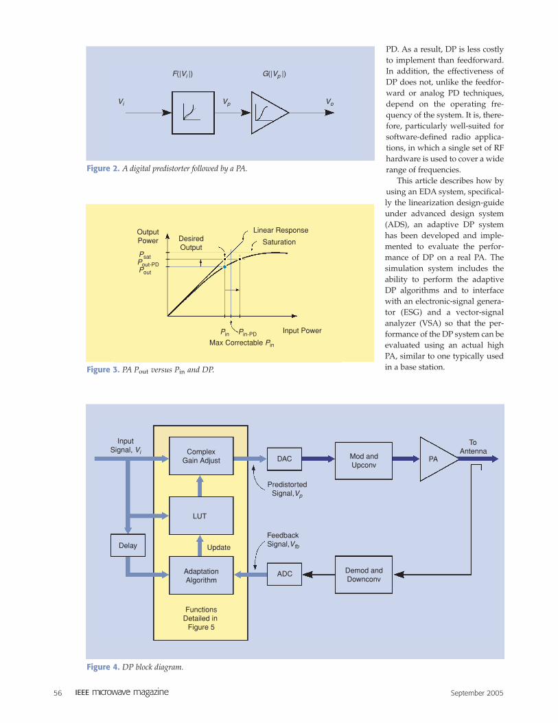
This article describes how byusing an EDA system, specifical-ly the linearization design-guideunder advanced design system(ADS), an adaptive DP systemhas been developed and imple-mented to evaluate the perfor-mance of DP on a real PA. Thesimulation system includes theability to perform the adaptiveDP algorithms and to interfacewith an electronic-signal genera-tor (ESG) and a vector-signalanalyzer (VSA) so that the per-formance of the DP system can beevaluated using an actual highPA, similar to one typically usedin a base station.Figure 3. PA Pout versus Pin and DP.
OutputPower
Input Power
Max Correctable Pin
DesiredOutput
Linear Response
Saturation
Psat
Pin Pin-PD
Pout-PDPout
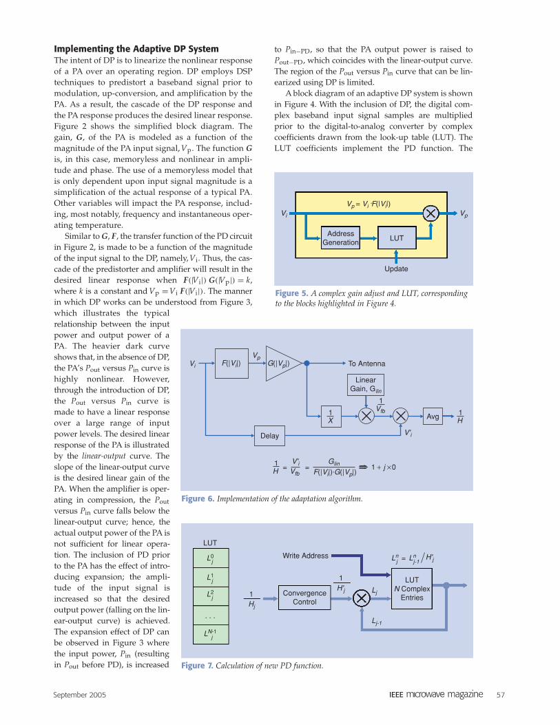
Figure 4. DP block diagram.
Functions Detailed in
Figure 5
Adaptation Algorithm
LUT
Feedback Signal,Vfb
Predistorted Signal,Vp
Complex Gain Adjust
Update
ADC
DAC
Demod and Downconv
Mod and Upconv
PA
ToAntenna
Delay
Input Signal, Vi
Figure 2. A digital predistorter followed by a PA.
Vi
F(|Vi |) G(|Vp |)
Vp Vo
September 2005 57
Implementing the Adaptive DP SystemThe intent of DP is to linearize the nonlinear responseof a PA over an operating region. DP employs DSPtechniques to predistort a baseband signal prior tomodulation, up-conversion, and amplification by thePA. As a result, the cascade of the DP response andthe PA response produces the desired linear response.Figure 2 shows the simplified block diagram. Thegain, G, of the PA is modeled as a function of themagnitude of the PA input signal, Vp. The function Gis, in this case, memoryless and nonlinear in ampli-tude and phase. The use of a memoryless model thatis only dependent upon input signal magnitude is asimplification of the actual response of a typical PA.Other variables will impact the PA response, includ-ing, most notably, frequency and instantaneous oper-ating temperature.
Similar to G, F, the transfer function of the PD circuitin Figure 2, is made to be a function of the magnitudeof the input signal to the DP, namely, Vi. Thus, the cas-cade of the predistorter and amplifier will result in thedesired linear response when F(|Vi|) G(|Vp|) = k,where k is a constant and Vp =Vi F(|Vi|). The mannerin which DP works can be understood from Figure 3,which illustrates the typicalrelationship between the inputpower and output power of aPA. The heavier dark curveshows that, in the absence of DP,the PA’s Pout versus Pin curve ishighly nonlinear. However,through the introduction of DP,the Pout versus Pin curve ismade to have a linear responseover a large range of inputpower levels. The desired linearresponse of the PA is illustratedby the linear-output curve. Theslope of the linear-output curveis the desired linear gain of thePA. When the amplifier is oper-ating in compression, the Pout
versus Pin curve falls below thelinear-output curve; hence, theactual output power of the PA isnot sufficient for linear opera-tion. The inclusion of PD priorto the PA has the effect of intro-ducing expansion; the ampli-tude of the input signal isincreased so that the desiredoutput power (falling on the lin-ear-output curve) is achieved.The expansion effect of DP canbe observed in Figure 3 wherethe input power, Pin (resultingin Pout before PD), is increased
to Pin−PD, so that the PA output power is raised toPout−PD, which coincides with the linear-output curve.The region of the Pout versus Pin curve that can be lin-earized using DP is limited.
A block diagram of an adaptive DP system is shownin Figure 4. With the inclusion of DP, the digital com-plex baseband input signal samples are multipliedprior to the digital-to-analog converter by complexcoefficients drawn from the look-up table (LUT). TheLUT coefficients implement the PD function. The
Figure 5. A complex gain adjust and LUT, correspondingto the blocks highlighted in Figure 4.
Address Generation LUT
Update
VpVi
Vp = Vi F(|Vi|) .
Figure 6. Implementation of the adaptation algorithm.
Delay
LinearGain, GIin
Avg
To AntennaVi
Vp
V'i
F(|Vi|) G(|Vp|)
1H
1Vfb1
X
F(|Vi|) G(|Vp|)1H
V'iVfb
GIin= = 1 j 0+ ×
Figure 7. Calculation of new PD function.
ConvergenceControl
LUTN Complex
Entries
Write Address
LUT
L j1
L j0
L j2
LN-1j
. . .
1
1H'j
Lj-1
Lj
Hj
Lnj-1Ln
jH'j=
58 September 2005
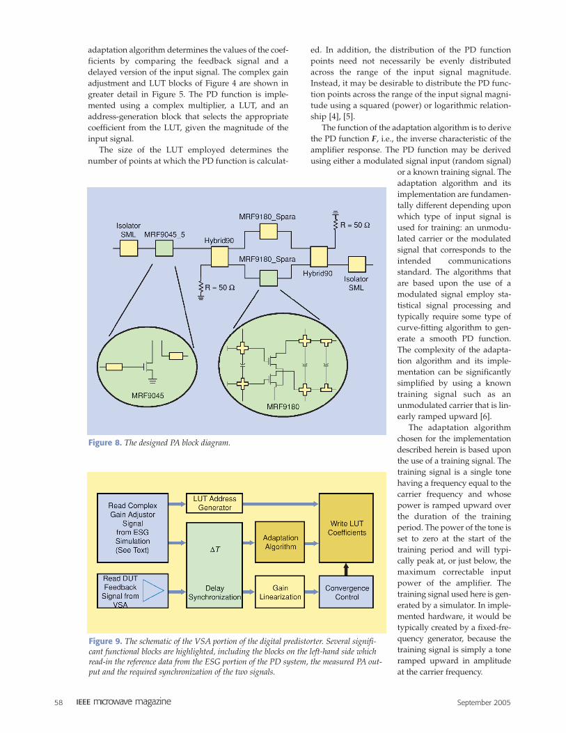
adaptation algorithm determines the values of the coef-ficients by comparing the feedback signal and adelayed version of the input signal. The complex gainadjustment and LUT blocks of Figure 4 are shown ingreater detail in Figure 5. The PD function is imple-mented using a complex multiplier, a LUT, and anaddress-generation block that selects the appropriatecoefficient from the LUT, given the magnitude of theinput signal.
The size of the LUT employed determines thenumber of points at which the PD function is calculat-
ed. In addition, the distribution of the PD functionpoints need not necessarily be evenly distributedacross the range of the input signal magnitude.Instead, it may be desirable to distribute the PD func-tion points across the range of the input signal magni-tude using a squared (power) or logarithmic relation-ship [4], [5].
The function of the adaptation algorithm is to derivethe PD function F, i.e., the inverse characteristic of theamplifier response. The PD function may be derivedusing either a modulated signal input (random signal)
or a known training signal. Theadaptation algorithm and itsimplementation are fundamen-tally different depending uponwhich type of input signal isused for training: an unmodu-lated carrier or the modulatedsignal that corresponds to theintended communicationsstandard. The algorithms thatare based upon the use of amodulated signal employ sta-tistical signal processing andtypically require some type ofcurve-fitting algorithm to gen-erate a smooth PD function.The complexity of the adapta-tion algorithm and its imple-mentation can be significantlysimplified by using a knowntraining signal such as anunmodulated carrier that is lin-early ramped upward [6].
The adaptation algorithmchosen for the implementationdescribed herein is based uponthe use of a training signal. Thetraining signal is a single tonehaving a frequency equal to thecarrier frequency and whosepower is ramped upward overthe duration of the trainingperiod. The power of the tone isset to zero at the start of thetraining period and will typi-cally peak at, or just below, themaximum correctable inputpower of the amplifier. Thetraining signal used here is gen-erated by a simulator. In imple-mented hardware, it would betypically created by a fixed-fre-quency generator, because thetraining signal is simply a toneramped upward in amplitudeat the carrier frequency.
Figure 8. The designed PA block diagram.
Figure 9. The schematic of the VSA portion of the digital predistorter. Several signifi-cant functional blocks are highlighted, including the blocks on the left-hand side whichread-in the reference data from the ESG portion of the PD system, the measured PA out-put and the required synchronization of the two signals.
September 2005 59
However, the use of the training signal does requirethat the modulated signal be interrupted while thetraining signal is transmitted. In addition, since thetraining signal is a single tone, the digital predistorteris only correcting for the operation of the amplifier at asingle frequency, not across the entire transmissionbandwidth. If the amplifier’s passband is quite flat, theuse of a single-tone training signal in this manner willenable the PD function to be determined accurately. Inany event, the use of a single complex coefficient tocorrect for distortion of the amplifier at a particularpower level presupposes that any amplifier memoryeffects are minimal.
Figure 6 shows a block diagram of the adaptationalgorithm that is employed. The algorithm is basedupon the determination of the open loop gain H, of thepredistorter and amplifier combination, at the powerlevel associated with each LUT entry. Recall that thedesired linear response of the predistorter and amplifiercascade requires that F(|Vi|) G(|Vp|) = k for all inputs.Hence, if Glin is set to be equal to k, the desired open-loop gain of the system is unity. Glin is a constant valueafter linearization. If the calculated open-loop gain isnot equal to unity, the PD function must be adjusted ina manner to drive the open loop towards unity. Thiscan be achieved in the manner illustrated in Figure 7.
The PD function is defined by a set of coefficientsstored in the LUT, Ln, where each n corresponds to aninput-signal magnitude that is mapped to an LUTaddress. In order to drive the open-loop gain to unity,the PD function’s coefficients are updated by dividingeach coefficient by the calculated open-loop gain.
The delay in the feedback path is estimated by calcu-lating the correlation between the magnitude of theinput signal and the magnitude of the feedback signal.
The use of the magnitude of the signals has the benefitof not requiring phase synchronization in the feedbackpath. Since the delay in the feedback path will not nec-essarily be equal to an integer number of DSP sampleperiods, interpolation is employed to more preciselyalign the input and feedback signals. The correlationbetween the input and feedback signal is performed ona modulated signal that precedes the training signalbecause the gain compression of the amplifier makesthe accuracy of the correlation over the training signalsuspect. In general, the accuracy of the estimationimproves as the block size increases. Unfortunately, alarger block size requires more memory and takeslonger to adapt.
The PD function cannot be exactly determined fol-lowing the transmission of a single training ramp andrequires an iterative calculation of the LUT coefficients.
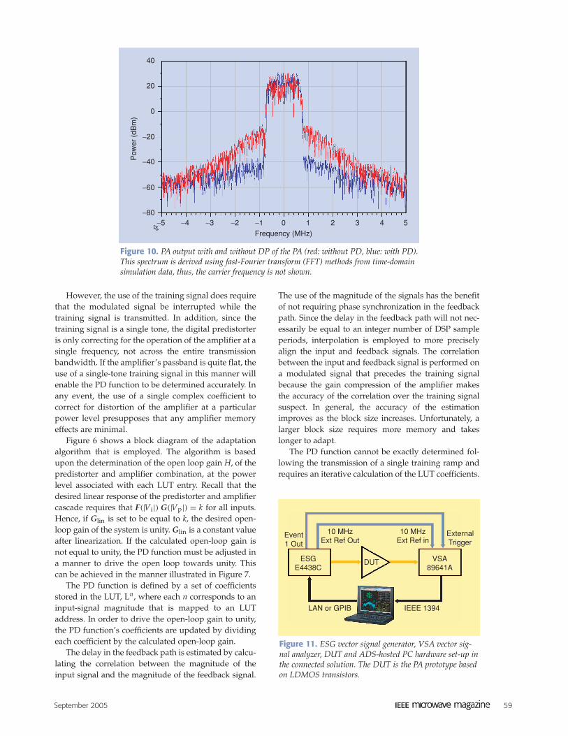
Figure 10. PA output with and without DP of the PA (red: without PD, blue: with PD).This spectrum is derived using fast-Fourier transform (FFT) methods from time-domainsimulation data, thus, the carrier frequency is not shown.
−5−80
−60
−40
−20P
ower
(dB
m)
0
20
40
−4 −3 −2 −1 0
Frequency (MHz)
4321 5
Figure 11. ESG vector signal generator, VSA vector sig-nal analyzer, DUT and ADS-hosted PC hardware set-up inthe connected solution. The DUT is the PA prototype basedon LDMOS transistors.
Event1 Out
ExternalTrigger
ESGE4438C
DUT
10 MHzExt Ref Out
10 MHzExt Ref in
LAN or GPIB IEEE 1394
VSA89641A
60 September 2005
A series of training ramps will have to be transmitted—although, in practice, significant improvements in theACPR of the amplifier are often observed even afterjust two or three training ramps.
The Connected SolutionThe use of a mixed software-hardware design methodmay be referred to as a “connected solution.” The tra-ditional design methodology for modern communica-
tion systems typically starts with the use of EDA toolsto develop an initial design from functional blocks andmodels. The behavior of the design is then studied byexecuting a multitude of different simulations.Modifications to the design are made within the EDAenvironment until acceptable performance is achieved.A prototype based upon the EDA-developed design isfabricated and evaluated within the laboratory setting.Commonly, at this hardware measurement stage, unex-pected issues arise due to imperfections in the modelsand information used during the design phase.
An alternative to the traditional design methodologythat does not separate the EDA and laboratory phasesof system development can be advantageous for anumber of reasons. By combining EDA tools withinstrumentation, flexible verification solutions can becreated to meet emerging requirements not met byinstruments or EDA alone. In addition, the more mea-surements added to a simulation, the more realisticand predictive are the results. As more realistic, com-plex, and custom signals and measurements are gen-erated and/or recovered in the EDA environment, thegreater the insight into the performance of a deviceunder test (DUT). Moreover, the speed of the designprocess may be increased as hardware-related issuesare uncovered sooner and more easily analyzed in thecontext of the system.
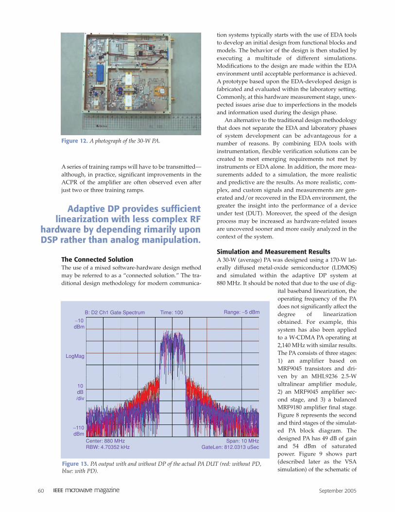
Simulation and Measurement ResultsA 30-W (average) PA was designed using a 170-W lat-erally diffused metal-oxide semiconductor (LDMOS)and simulated within the adaptive DP system at 880 MHz. It should be noted that due to the use of dig-
ital baseband linearization, theoperating frequency of the PAdoes not significantly affect thedegree of linearizationobtained. For example, thissystem has also been appliedto a W-CDMA PA operating at2,140 MHz with similar results.The PA consists of three stages:1) an amplifier based onMRF9045 transistors and dri-ven by an MHL9236 2.5-Wultralinear amplifier module,2) an MRF9045 amplifier sec-ond stage, and 3) a balancedMRF9180 amplifier final stage.Figure 8 represents the secondand third stages of the simulat-ed PA block diagram. Thedesigned PA has 49 dB of gainand 54 dBm of saturatedpower. Figure 9 shows part(described later as the VSAsimulation) of the schematic of
Figure 12. A photograph of the 30-W PA.
Figure 13. PA output with and without DP of the actual PA DUT (red: without PD,blue: with PD).
Span: 10 MHzGateLen: 812.0313 uSec
Center: 880 MHzRBW: 4.70352 kHz
Time: 100
LogMag
−10dBm
10dB/div
−110dBm
B: D2 Ch1 Gate Spectrum Range: −5 dBm
Adaptive DP provides sufficientlinearization with less complex RF
hardware by depending rimarily uponDSP rather than analog manipulation.
September 2005 61
the designed digital predistorter. All subsystems dis-cussed under the heading “Adaptive DP System” wereimplemented within the ADS Ptolemy environment.ADS Ptolemy provides a set of DSP and RF modelblocks and supports simulation of mixed baseband andmodulated RF signals, a requirement for DP. Figure 10illustrates the simulation results; approximately 20 dBof distortion correction is achieved at the 45 W outputpower level.
Figure 11 illustrates the set-up for interconnectingthe vector signal generator, amplifier (which is theDUT), vector signal analyzer, and the digital predis-torter system design. The DUT is the 30-W (average)LDMOS PA (Figure 12) as described above. The processof linearization consists of two separate steps, herereferred to as: 1) ESG simulation and 2) VSA simula-tion. We use the term “simulation” not in the experi-mental sense but to recognize that a simulation tool isbeing used to implement the DSP portions of the sys-tem. However, the same algorithms may be configuredin a pure simulation mode using a model of the PA. Inthis way, the design may be first predicted using simu-lation only but then verified and improved using theconnected mode with the real PA hardware. The ESGsimulation generates and predistorts the modulatedsignal, passing it on to the ESG, where the signal ismodulated onto an RF carrier. The RF output of theESG is fed to an amplifier, the output of which is con-nected to the VSA through an attenuator to protect theVSA’s input circuitry. The VSA captures the downcon-verted signal and transfers the signal into the ADSdomain, whereby ADS performs signal processing toupdate the set of LUT coefficients. A CDMA2000 mod-ulated signal with 1.2288-MHz chip rate and 9.6 dB ofpeak-to-average ratio (PAR) was used for the simula-tions and measurements. Figure 13 shows the PA out-put with DP applied after three iterations at 45 W ofoutput power. The out-of-band spectra were reducedby over 15 dB, as seen by comparing the blue tracerepresenting the output signal with PD to the red trace,which is the uncorrected output. Compared to the sim-ulation results, a 5-dB difference was observed. Thisdiscrepancy may be due to temperature-based memoryeffects, the limit on the VSA’s bandwidth (36 MHz),and/or inaccuracies of the active device’s “Root”model used for simulation.
Although this article focuses on adaptive digital lin-earization using a simple training signal for correctingonly memoryless nonlinearities of a PA, understandingthe effects of the system’s bandwidth is valuable whenimplementing practical linearized amplifiers. Band-width limitations, for instance, may depend on thewireless system’s ACPR specification. For adequate
cancellation of distortion products, the digital predis-torter should consider the fifth order IMD products ofthe PA under consideration. For example, if the signalbandwidth is 10 MHz, the DSP bandwidth should be 50MHz. Moreover, memory effects limit the performanceof DP, because memory effects become significant assignal bandwidth increases.
ConclusionsWhen compared to other linearization methods, adap-tive DP provides sufficient linearization with less com-plex RF hardware by depending primarily upon DSPrather than analog manipulation. The adaptive DP sys-tem may be implemented in EDA software along withinterconnected test equipment (arbitrary RF signalsource and vector signal analyzer). Through the use ofa training signal, a simple adaptive algorithm may beemployed to update the LUT coefficients until an opti-mum setting is achieved and used to predistort theinput to the amplifier. This “connected solution”approach can provide key information to design engi-neers for optimizing the DSP architecture of a PA. Forfuture work, other issues will be taken into account,such as temperature and electrical memory effects.
References[1] D. Hilborn, S.P. Stapleton, and J.K. Cavers, “An adaptive direct
conversion transmitter,” IEEE Trans. Veh. Technol., vol. 43, pp.223–233, May 1994.
[2] O. Ichiyoshi, “High-power linear amplification using periodicallyupdated amplitude and phase correction values,” U.S. Patent 5699 383, Dec. 16, 1997.
[3] F. Zavosh, M. Thomas, C. thron, T. Hall, D. Artusi, D. Anderson,D. Ngo, and D. Runton, “Digital predistortion techniques for RFpower amplifiers with CDMA applications,” Microw. J., Oct. 1999.
[4] “Adaptive predistortion using the ISL5239,” Intersil ApplicationNote AN1028, Sept. 2002.
[5] K.J. Muhonen, M. Kavehrad, and R. Krishnamoorthy, “Look-uptable techniques for adaptive digital predistortion: A developmentand comparison,” IEEE Trans. Veh. Technol., vol. 49, pp. 1995–2002,Sept. 2000.
[6] J. de Mingo and A. Valdovinos, “Performance of a new digitalbaseband predistorter using calibration memory,” IEEE Trans. Veh.Technol., vol. 50, pp. 1169–1176, July 2001.
A simple adaptive algorithm may beemployed to update the LUTcoefficients until an optimum settingis achieved and used to predistortthe input to the amplifier.